Silicon is the king of semiconductor materials. For many years this material has been used to manufacture electronic devices of all types. Transistors, microcontrollers, sensors, you name it! There are many reasons for this: silicon is the second most abundant material on the face of the earth, its melting point is high enough so that thermal processes in the cleanroom do not melt it, it has a moderate band gap of 1.1 eV that allows for low-voltage operation with small leakage current, and other attributes. One of these attributes – one of the most important features for using silicon – is the fact that when exposed to oxygen (“rust”) it forms a “native” outstanding insulator and protector, silicon dioxide (SiO2), that is essential during the manufacturing process of chips.
The large 9.0 eV band gap of SiO2 and its high compatibility with silicon are perhaps the most important features in relation to enabling the isolation of silicon components and the reduction of leakage current. We have not been able to replicate the combination of the 1.1 eV gap of silicon and the large gap of its native insulator in other semiconductor materials, such as germanium or compound III-V materials, despite our long years of research. Other than silicon, semiconductor materials must be “supplied” (deposited) externally with the needed layers of insulation material.
Silicon, however, is not perfect. Nowadays we are running to keep shrinking the size of the chips day by day, but silicon has not been able to follow the trend. By decreasing the size of the transistors, the size of the gate silicon dioxide (the insulator between the gate and the channel) has been decreasing as well. But the smaller the gate oxide the bigger the capacitance between the gate and the channel; this, in turn, dramatically increases the undesirable leakage current and thus more power is needed to drive the transistor.
So the solution is to replace the SiO2 in the gate with an insulator with a high dielectric constant (high-k) in order to be able to reduce the capacitance of the gate-channel (to reduce the leakage current). With a high-k insulator, we can afford a thicker gate insulator, as is indicated in the figure. This task has been under the radar of the research community for a long time now. The idea is to be able to shrink the size of the transistors without increasing the leakage current.
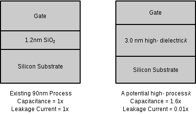 Conventional silicon dioxide gate dielectric structure compared to a potential high-k dielectric structure. Image credit: Wikipedia.
A team of engineers at Stanford University have, finally, identified two possible new materials--hafnium diselenide (HfSe2) and zirconium diselenide (ZrSe2)--that can be used to replace silicon. On August 11, 2017, professor Eric Pop and post-doctoral student Michal Mleczko published their research efforts in the journal Science Advances. The two materials can produce native oxides (“rust”) and at the same time, the “rust” exhibits a high-k dielectric. "It's a bit like rust, but a very desirable rust," said Eric Pop. The new materials can also be scaled down to three atoms thick to create the chip components.
"Engineers have been unable to make silicon transistors thinner than about five nanometers before the material properties begin to change in undesirable ways," Pop said. Being able to create thinner circuits and insulators with desirable high-k will extend the so call Moore’s Law by creating transistors ten times smaller than existing ones.
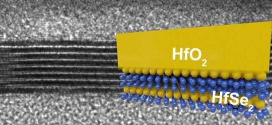 In this greatly enlarged cross-section of an experimental chip, the bands of black and white reveal alternating layers of hafnium diselenide – an ultra thin semiconductor material – and the hafnium dioxide insulator. The cross-section matches an overlaid color schematic on the right. Credit: Michal Mleczko
"Silicon won't go away. But for consumers, this could mean much longer battery life and much more complex functionality if these semiconductors can be integrated with silicon," Pop said.
There is much to do, however, before we can see actual devices being manufactured with these two new 2-D materials. First, the researchers must refine the electrical contacts between transistors on the ultra thin diselenide circuits. "These connections have always proved a challenge for any new semiconductor, and the difficulty becomes greater as we shrink circuits to the atomic scale," Mleczko said. Another difficult task is to be able to “control” the high-k insulators to ensure they remain thin and stable after the manufacturing process.
"There's more research to do, but a new path to thinner, smaller circuits -- and more energy-efficient electronics -- is within reach," Pop said.
